Tungsten Selenide 08: FTO substrate WSe2 | Обустройство дома


Сохраните в закладки:

Цена:US $512.00RUB
*Стоимость могла изменится

Количество:


Новое поступление

Advanced 2D Materials CO.,Ltd Store

Advanced 2D Materials CO.,Ltd Store

Магазина Advanced 2D Materials CO.,Ltd Store работает с 04.12.2018. его рейтинг составлет 100 баллов из 100. В избранное добавили 353 покупателя. Средний рейтинг торваров продавца 4.8 в продаже представленно 1617 наименований товаров, успешно доставлено 52 заказов. 4 покупателей оставили отзывы о продавце.

Характеристики

Tungsten Selenide 08: FTO substrate WSe2 | Обустройство дома

История изменения цены

*Текущая стоимость US $512.00 уже могла изменится. Что бы узнать актуальную цену и проверить наличие товара, нажмите "Добавить в корзину"

Месяц Минимальная цена Макс. стоимость Цена
Mar-28-2026 609.60 руб. 639.53 руб. 624 руб.
Feb-28-2026 604.15 руб. 634.26 руб. 619 руб.
Jan-28-2026 507.4 руб. 532.51 руб. 519.5 руб.
Dec-28-2025 594.84 руб. 624.40 руб. 609 руб.
Nov-28-2025 517.47 руб. 543.95 руб. 530 руб.
Oct-28-2025 584.60 руб. 613.74 руб. 598.5 руб.
Sep-28-2025 579.96 руб. 608.49 руб. 593.5 руб.
Aug-28-2025 573.70 руб. 602.50 руб. 587.5 руб.
Jul-28-2025 568.87 руб. 596.66 руб. 582 руб.

Описание товара

Tungsten Selenide 08: FTO substrate WSe2 | Обустройство дома


The largest 4 inch discs are currently available, and larger sizes (8, 12 inches) are coming soon.   Production method: Chemical Vapor Deposition (CVD)   Product introduction: Six carbon technology WSe2 films are divided into a variety of: 1) A single layer of discretely distributed triangular single crystal grains having a triangular side length of typically several tens to one hundred micrometers. 2) A single-layer continuous film that continues to grow in Dalian by triangular grains. 3) Multilayer WSe2 continuous film. 4) Substrate: There are many alternative substrates for WSe2, and the sapphire substrate is a direct deposition product. Other substrates such as SiO2/Si, silicon wafers, PET, PI, ITO, FTO, glass, metal substrates, etc. are transferred to the substrate required by the customer after growth on sapphire.   Application areas: Optoelectronic devices, microelectronic devices, biosensing, chemical sensing and other fields.   Packaging and specifications 10*10mm, 15*15mm, 20*20mm, 2-inch wafer, 4-inch wafer or customer-specified custom size. Purification vacuum packaging, 1 piece / box, 5 pieces / box. 10 pieces / box.   Typical customers include: MIT, Caltech, Stanford University; Oxford University, Manchester University; Seoul National University, Korea Institute of Science and Technology (KAIST), and Sungkyunkwan University; Tokyo Institute of Technology, Murata Manufacturing Co., Ltd. Tsinghua University, Peking University, Institute of Semiconductors, Chinese Academy of Sciences And other world-class research institutions.

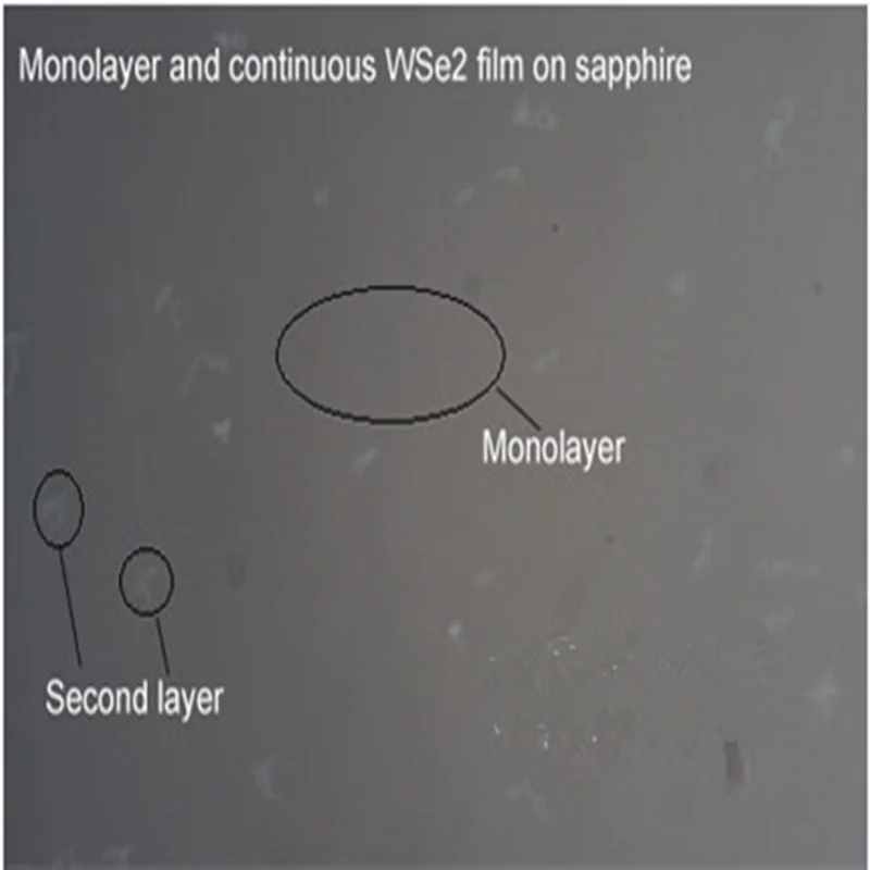
Single layer WSe2 isolated grain                                              Single layer WSe2 continuous film  

Monolayer-triangle-WSe2__ABUIABACGAAg4vHm0gUo2LOOuwMwuwM4rwI_1_


Single double layer hybrid WSe2

WSe2-2__ABUIhffKBxACGAAg5O7m0gUo1dfiiwEwrgQ4iwM___

ABUIhffKBxACGAAg5O7m0gUouNKNZTCuBDiLAw___


Смотрите так же другие товары: