GM7123 VGA video module connected to fpga development board camera coms | Инструменты


Сохраните в закладки:

Цена:979,17RUB
*Стоимость могла изменится

Количество:


Новое поступление

Going Up Store

Going Up Store

Магазина Going Up Store работает с 20.05.2018. его рейтинг составлет 91.73 баллов из 100. В избранное добавили 1475 покупателя. Средний рейтинг торваров продавца 4.7 в продаже представленно 4520 наименований товаров, успешно доставлено 3008 заказов. 786 покупателей оставили отзывы о продавце.

Характеристики

GM7123 VGA video module connected to fpga development board camera coms | Инструменты

История изменения цены

*Текущая стоимость 979,17 уже могла изменится. Что бы узнать актуальную цену и проверить наличие товара, нажмите "Добавить в корзину"

Месяц Минимальная цена Макс. стоимость Цена
Feb-28-2026 1243.93 руб. 1268.18 руб. 1255.5 руб.
Jan-28-2026 1008.14 руб. 1028.10 руб. 1018 руб.
Dec-28-2025 1224.48 руб. 1248.16 руб. 1236 руб.
Nov-28-2025 1214.95 руб. 1238.76 руб. 1226 руб.
Oct-28-2025 969.95 руб. 988.63 руб. 978.5 руб.
Sep-28-2025 1194.31 руб. 1218.40 руб. 1206 руб.
Aug-28-2025 1185.64 руб. 1209.1 руб. 1197 руб.
Jul-28-2025 1175.64 руб. 1199.20 руб. 1187 руб.

Описание товара

GM7123 VGA video module connected to fpga development board camera coms | ИнструментыGM7123 VGA video module connected to fpga development board camera coms | ИнструментыGM7123 VGA video module connected to fpga development board camera coms | Инструменты


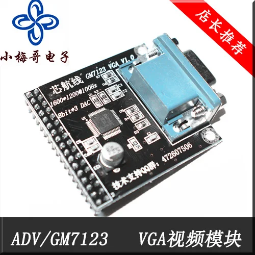
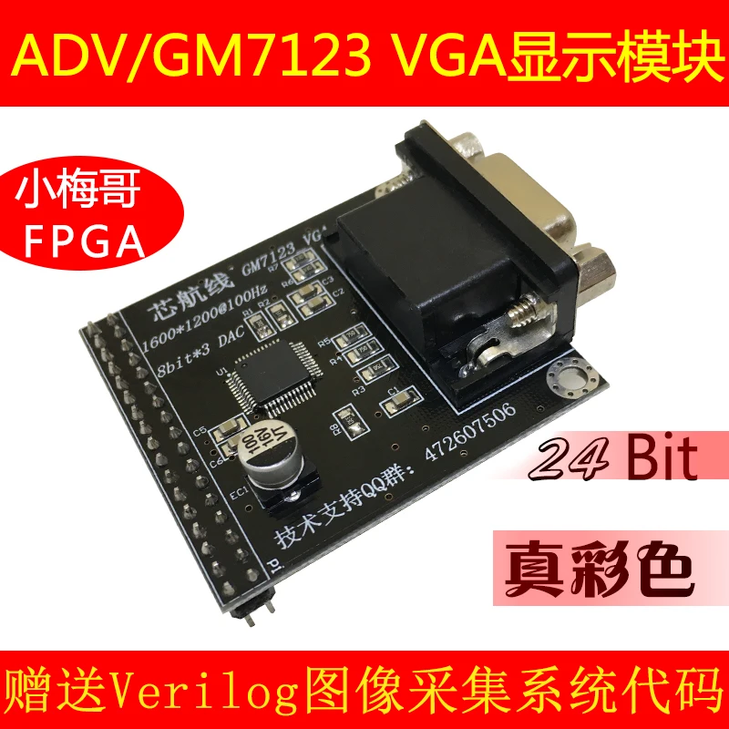
Update notification:   The new version of this module has been changed to black solder mask, the effect is better. All customers who place orders will be issued a black version. The black and red hardware circuits and wiring are exactly the same, only the printed color of the PCB is modified, so please feel free to purchase.    


note:     The module uses the GM7123 chip, which has the same parameters and performance as the ADV7123 chip.     Quality function: The GM7123 is a 330MHz 3-channel 10-bit high-speed video DAC chip that is compatible with the RS-343A/RS-170 standard differential outputs and has an output current range of 2mA to 26mA. The input is compatible with TTL levels, an internal reference of 1.23V, and a single-supply 3.3V supply in an LQFP48 package. The GM7123 comes with 3 separate 10-bit data input ports with video control signals SYNC and BLANK to control synchronization and blanking, respectively. Manufactured in a CMOS process. Functional and pin compatible with the ADV7123.   a) 330MSPS conversion rate   b) 3 10-bit DACs   c) Input compatible TTL level   d) DAC output current range 2mA ~ 26mA   e) Integrated bandgap reference   f) LQFP48 package   Difference between GM7123 and ADV7123 voltage The ADV7123's power supply voltage is compatible with 5V/3.3V   The GM7123's supply voltage only supports 3.3V.   Standby power supply current The standby supply current of the ADV7123 is typically about 2mA.   The GM7123's standby supply current is typically about 0.2mA.       The schematic diagram of the core route GM7123 VGA output module is as follows   Use points Precautions To connect a standard VGA monitor output VGA image using the ADV/GM7123 module, the following points must be met:   1, VGA_VS, VGA_HS meet various standard VGA timing standards. A standard VGA timing, in addition to the data segment, there are blanking segments and sync segments, so these two signals must be set to fully comply with the standard VGA timing. Otherwise the display will not be recognized and displayed properly.   2. The CLOCK signal must meet the 60Hz refresh rate request. For example, for a resolution of 800*600@60Hz, the CLOCK signal must be around 40MHz, allowing for very small deviations, such as 39.2MHz, but not too much, for example, giving a 30MHz clock signal. , the display will not be recognized and displayed.   3, VGA interface does not support a variety of other non-standard timing, such as 30 frames, 20 frames and other LCD can support the refresh rate. In order to output higher resolution images, some MCUs have a lower refresh rate, and some even as low as 5 frames. This way, the RGB interface can be supported in front of the LCD, but this is impossible for the VGA interface to display.   4. The BLK signal must be connected. For some processors or MCUs with LCD drivers, connect this signal to the DE pin of the LCD driver of the processor.   5. If the BLK signal cannot be generated, the BLK signal can be directly connected to the high level, and during the Blank period, the data on the RGB data line is controlled to be 0.   6. If the display content appears partially blooming, the typical phenomenon is that some abnormal colors appear in the image where the chromaticity changes greatly. This is often because the CLOCK trace and the data line trace length of the driver (MCU or FPGA) are different. Larger, the CLOCK signal can be inverted (inverted), or the timing constraint can be used to adjust the delay of the data line relative to the CLOCK signal.       The GM7123 VGA output module only implements digital signal-to-analog functions. It cannot perform any communication protocol conversion, nor can it generate any timing signals, and can be used without any configuration. Therefore, it is only necessary to design the drive logic according to the labeled VGA timing. For the design of the VGA driver, please refer to the article about Xiaomei.       (Note: The names of the module-derived signals described in RGB[7..0] below, not the chip pin names)       RGB888 connection When using the RGB888 interface timing, connect as follows.       RGB666 connection   When using RGB666 interface timing, only R[7..2], G[7..2], B[7..2] are used to connect RGB666 data, and R[1..0], G[1..0 ], B[1..0] is connected to GND (when the requirement is very low, it is also suspended, it does not affect the function, but it is not recommended). It can be connected as follows.      


RGB565 connection       When using RGB565 interface timing, only R[7..3], G[7..2], B[7..3] are used to connect RGB565 data, and R[2..0], G[1..0 ], B[2..0] is connected to GND (when the requirement is very low, it is also suspended, it does not affect the function, but it is not recommended). It can be connected as follows.      


RGB555 connection   When using RGB555 interface timing, only R[7..3], G[7..3], B[7..3] are used to connect RGB555 data, and R[2..0], G[2..0 ], B[2..0] is connected to GND (when the requirement is very low, it is also suspended, it does not affect the function, but it is not recommended). It can be connected as follows.    


The module selects the upper 8 bits of the three DAC channels of the GM7123 chip as the data input port, and the lower 2 bits are discarded. Therefore, the RGB888 format, which is 24-bit color, is supported by default. This graphics quality has fully met the PC display standard. This module introduces VGA_HS, VGA_VS, CLOCK, BLK (BLANK), R7~R0, G7~G0, B7~B0, 3.3V, GND signals to the user. For the user, just connect these signals correctly and give the correct VGA standard signal.   The module uses a 2*17 double-row pin interface, with the top left being 1 pin

Module details map reward:


 The following is an image display system designed by customers using LPC1788 plus our VGA module. The effect is good, the board making process is also good, and the visual inspection is engraved by the engraving machine. The resolution is 800*600.


Смотрите так же другие товары: